Advanced CMOS technology for high-end scientific imaging applications
TVIPS introduces a new generation of TEM cameras based on a custom designed CMOS architecture: TemCam-F816, TemCam-F416 and TemCam-F216. These cameras are featuring a large fill factor, a high sensitivity and a superior resolution hence combining the advantages of classical slow scan CCD cameras with an exceptional acquisition speed. TemCam-F816, TemCam-F416 and TemCam-F216 are fulfilling the advanced requirements for applications in both materials science and life sciences.
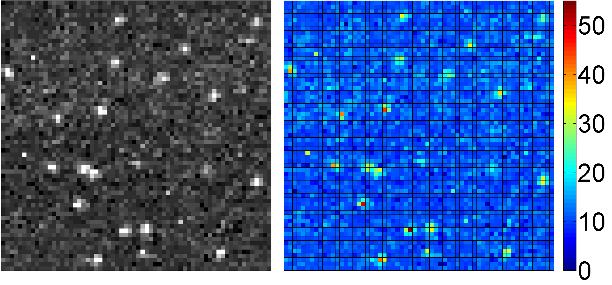 Latest improvements in CMOS process technology opened new possibilities for the design of highly accurate and ultra stable CMOS architectures. TVIPS uses lowest noise sensors for its cameras resulting in high dynamic range (>10,000:1) and single electron sensitivity.

Unlike CCDs, CMOS sensors do not show any blooming effects or smearing artifacts owing to intensive illumination or overexposure. This inherent ability renders them entirely suitable for all types of applications using high intensities such as recording diffraction patterns.
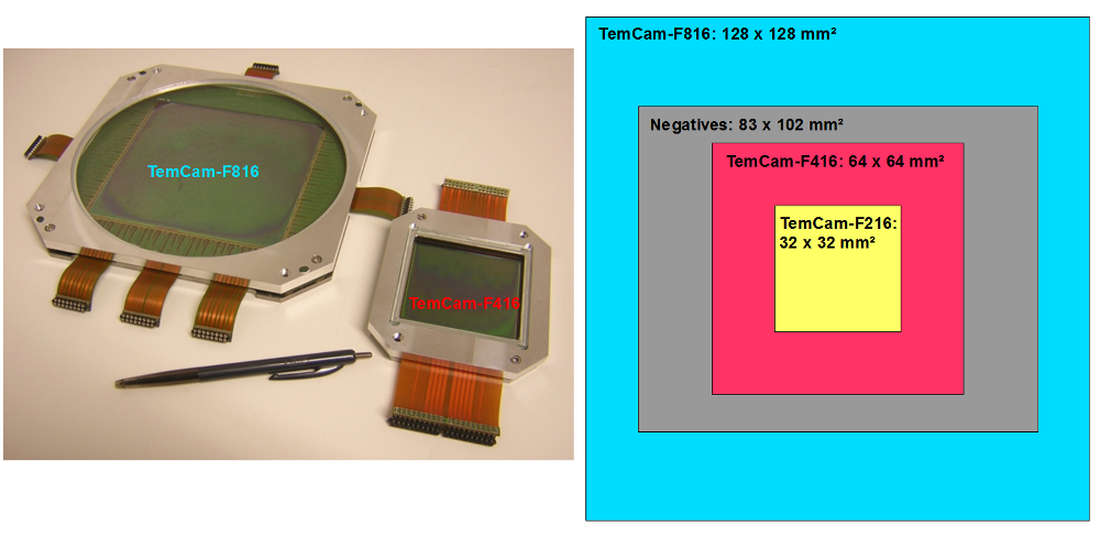 The combination of a large pixel size (15.6 µm) and advanced stitching technology leads to monolithic image sensor areas of up to 128 x 128 mm2 resulting in 64 MegaPixel.
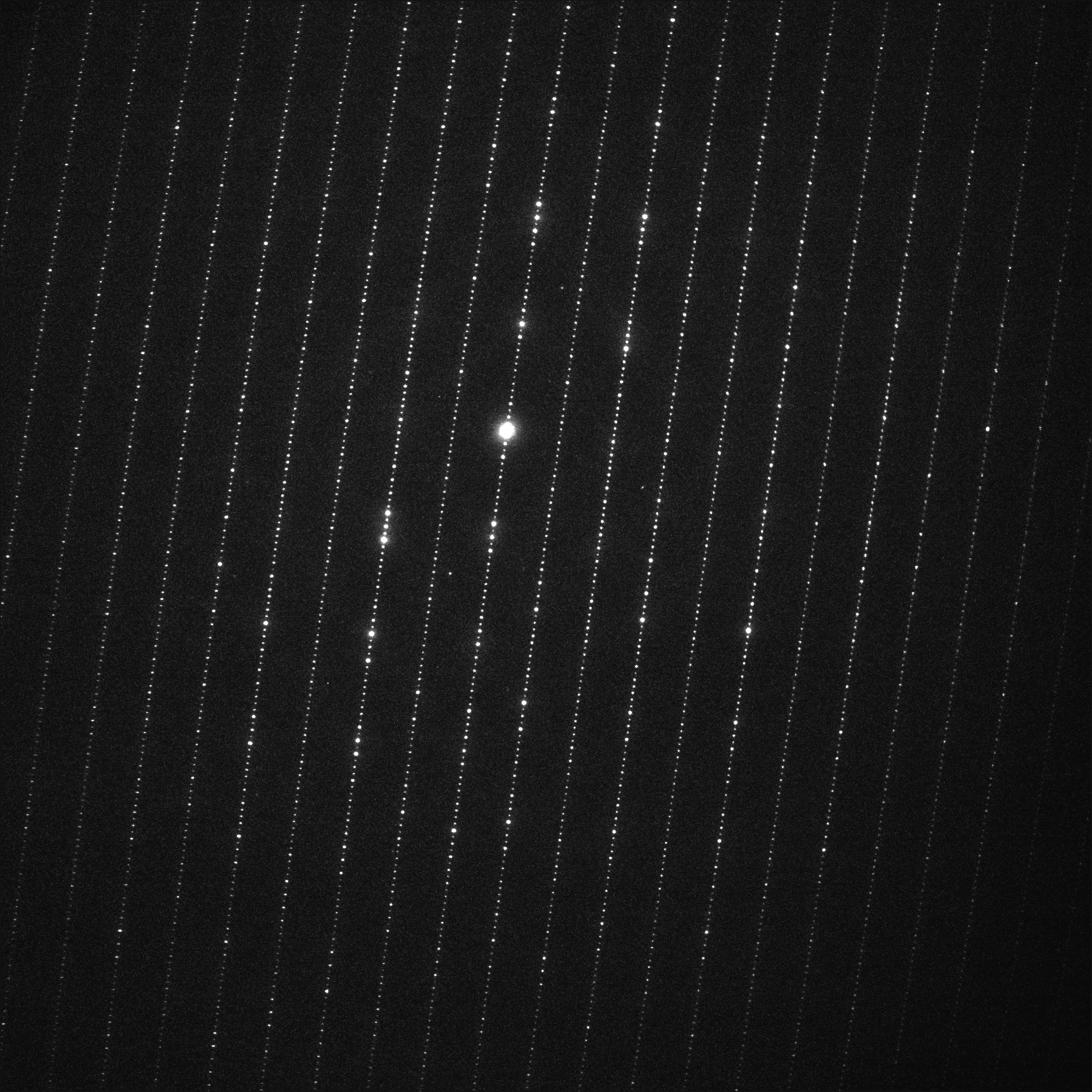
All TVIPS CMOS cameras use innovative readout techniques which allow addressing arbitrary subareas in 1k steps both in x- and y- direction. These special formats are beneficial for recording EELS spectra.

 10MHz+ design on up to 8 simultaneous readout channels increases overall speed to levels which have been limited to interline CCDs so far. The image sensor can be operated in the so called “Non Destructive Readout” (NDR) mode or in the “rolling shutter” (RS) mode. For low noise and high sensitivity single image acquisition, the NDR mode is used whereby the noise is reduced to a minimum similar to the typical read out noise of slow scan CCD cameras. The typical read out time of a 4k × 4k area is 1 second.
For an even faster read out a rolling shutter mode is available, enabling read-out rates of up-to 8.5fps without requiring a global shutter in the TEM.
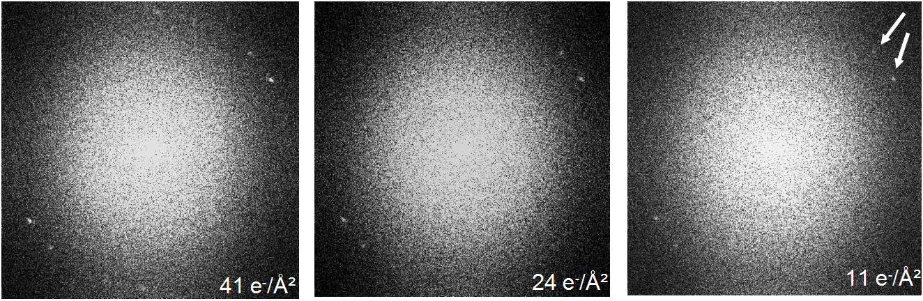
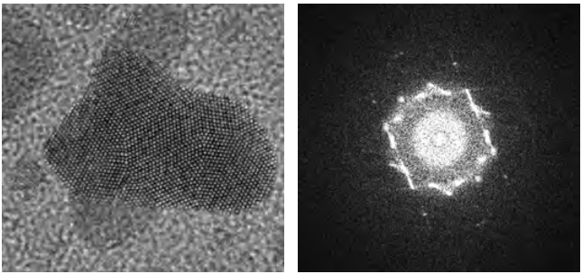
Several applications like cryo microscopy or investigation of beam-sensitive materials require high resolution images under low dose conditions in order to prevent radiation damage of those delicate samples.
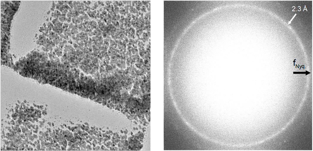
Cross grating replica with gold islands is an ideal test specimen for comparison of spatial resolution versus applied dose. Even under extreme low dose conditions the gold lines close to Nyquist frequency are clearly visible in the power spectrum.